File
Products
Installation
About
The PDS Accelerator Card transforms a Macintosh SE into a 32-bit workstation. A MC68030 CPU at 50 MHz, MC68882 FPU, and 64 MB of SDRAM — all on a single card that plugs into the SE's Processor Direct Slot.
No more choosing between speed and RAM. One slot, everything you need.
| CPU | MC68030RC50 @ 50 MHz, full 32-bit, on-chip MMU |
|---|---|
| FPU | MC68882RC50 @ 50 MHz (matched clock) |
| RAM | 64 MB SDRAM (2× IS42S16320F, 32-bit data path, burst mode) |
| Bus Logic | Lattice MachXO2-2000HC CPLD — bus arbitration, clock domain crossing, SDRAM controller |
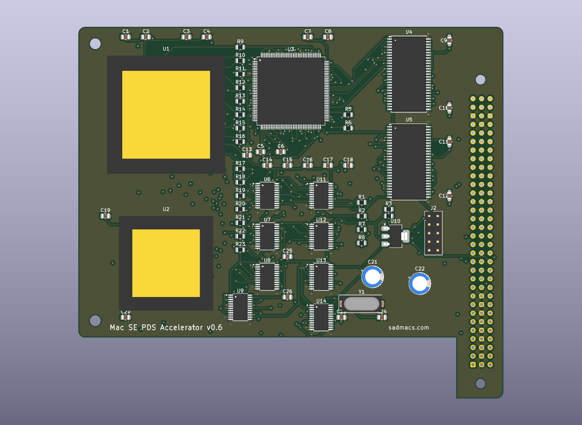
| Interface | 96-pin DIN41612 vertical female (Mac SE PDS, 3-row C type, B.Cu) |
| PCB | 112 × 92 mm, 6-layer (F.Cu / In1–In4 / B.Cu) |
| Level Shifting | 8× SN74LVC8T245 (5V PDS ↔ 3.3V CPU/CPLD) |
| Power | 3.3V LDO from PDS +5V rail |
| Clock | 50 MHz crystal oscillator + 8 MHz from PDS C8M |
| Programming | JTAG header for CPLD (2×5 pin, 2.54 mm) |
The CPLD implements full 68000-family bus arbitration. It asserts /BR (bus request) to the SE's onboard 68000, waits for /BG (bus grant), then acknowledges with /BGACK. The original 68000 is tri-stated while the 68030 runs. On PDS access (I/O, ROM), the 68030 relinquishes the bus back to the SE's native bus cycle.
The Mac SE runs at 8 MHz (C8M on PDS). The 68030 runs at 50 MHz from its own crystal. The CPLD synchronizes transfers between the two domains with proper handshaking and wait states — no metastability, no data corruption.
| Range | Size | Description |
|---|---|---|
| $00000000–$03FFFFFF | 64 MB | SDRAM (fast, 0 wait states at 50 MHz) |
| $40000000–$4FFFFFFF | — | PDS bus access (SE ROM, I/O — 8 MHz with wait states) |
| $50000000–$5000FFFF | 64 KB | CPLD register space |
The CPLD implements a full SDRAM controller: AUTO REFRESH every 7.8 µs, CAS latency 3, burst length 4. The 32-bit data path (two 16-bit ICs interleaved) feeds the 68030's data bus directly. Burst mode gives effective bandwidth of 200 MB/s peak.
| Ref | Component | Package | Est. Cost |
|---|---|---|---|
| U1 | MC68030RC50 | PGA-128 | $80–150 |
| U2 | MC68882RC50 | PGA-68 | $10–20 |
| — | PGA-128 socket (optional, for U1) | Machined pin | $10–30 |
| — | PGA-68 socket (optional, for U2) | Machined pin | $5–20 |
| U3 | MachXO2-2000HC | TQFP-144 | $8 |
| U4, U5 | IS42S16320F (32 MB each) | TSOP-II-54 | $3 ea |
| U6–U9, U11–U14 | SN74LVC8T245 level shifters | TSSOP-24 | $1 ea |
| U10 | AMS1117-3.3 LDO | SOT-223 | $0.30 |
| Y1 | 50 MHz crystal oscillator | HC49-SD | $0.50 |
| J1 | DIN41612 C 3×32 Female | Vertical THT | $5–10 |
| J2 | JTAG header 2×5 | 2.54 mm pin header | $0.20 |
| C1–C26 | Decoupling capacitors | 0805 + radial | $2 total |
| R1–R23 | Resistors (pull-ups, divider, series protection) | 0805 | $1 total |
| PCB fabrication (6-layer, JLCPCB) | $15–25 | ||
| Estimated Total | ~$130–250 | ||
The PCB supports both direct soldering and socketed installation for the CPU and FPU (1.0 mm drill holes, 2.54 mm pitch). Sockets are optional but recommended — they let you swap or reuse the chips later.
| Socket | Recommended Part | Source | Price |
|---|---|---|---|
| PGA-128 (U1) | Preci-Dip 510-87-128-13-041101 | Mouser, DigiKey | ~$10–15 |
| PGA-128 (U1) | Mill-Max 510-43-128-13-041001 | DigiKey, Mouser | ~$30 |
| PGA-68 (U2) | Mill-Max 510-93-068-10-041001 | Mouser | ~$15–20 |
| PGA-68 (U2) | Phoenix Enterprises HWS3728 | peconnectors.com | ~$2 |
6-layer board: signal/GND/signal/signal/power/signal. 112×92 mm with 2 mm corner radii. Card sits flat above the Mac SE logic board with vertical DIN41612 female connector on B.Cu (bottom side) plugging into the PDS slot. GND copper pours on front and back.
Design files (KiCad 10, Gerbers, BOM) available on Forgejo.
PCB design complete. Gerbers exported and ready for fabrication. Next steps: order boards from JLCPCB, source components, assemble prototype, write CPLD firmware.
Email rob@sadmacs.com to get notified when kits are available.